PCB antenna testing
Introduction
Printed circuit board (PCB) antennas have become popular because of their ease of design, small size, and low cost. PCB antennas have found applications in various devices, such as smartphones, tablets, laptops, wireless routers, and Internet of Things (IoT) devices. However, designing and testing PCB antennas is still a challenging task because of the complex behavior of electromagnetic waves and the influence of various factors, such as substrate material, antenna geometry, and surrounding environment. In this article, we will discuss the principles of PCB antennas, the factors that affect their performance, and the methods used to test their characteristics.
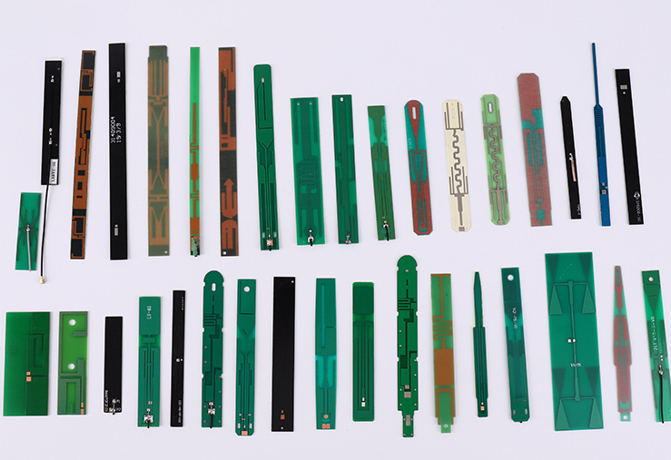
Principles of PCB Antennas
A PCB antenna is a microstrip antenna that uses a thin conductor on a dielectric substrate to radiate or receive electromagnetic waves. The basic structure of a PCB antenna consists of a metal patch (or several patches) on the top of the substrate and a ground plane (or several planes) on the bottom of the substrate, with a dielectric layer in between. The metal patch serves as the radiating element, while the ground plane provides a reference for the electric and magnetic fields. The dielectric layer acts as a medium for propagating the waves and controls the impedance and bandwidth of the antenna.
The design of a PCB antenna involves several parameters, such as the size, shape, and location of the metal patch, the thickness and permittivity of the dielectric layer, and the distance and dimensions of the ground plane. These parameters determine the resonance frequency, bandwidth, polarization, radiation pattern, and efficiency of the antenna. For example, a larger metal patch or a thinner dielectric layer can increase the radiation efficiency and bandwidth of the antenna, while a smaller ground plane or a thicker dielectric layer can reduce the radiation efficiency and bandwidth of the antenna.
Factors Affecting PCB Antenna Performance
The performance of a PCB antenna depends on several factors, such as the substrate material, the antenna geometry, the feeding mechanism, and the surrounding environment. These factors can affect the radiation efficiency, impedance matching, and bandwidth of the antenna, and can lead to detuning, distortion, or interference.
Substrate material: The choice of substrate material affects the dielectric constant, loss tangent, and thickness of the dielectric layer, which in turn affects the impedance and bandwidth of the antenna. Common substrate materials for PCB antennas are FR-4 epoxy, Rogers RT/Duroid, and Teflon.
Antenna geometry: The shape, size, and orientation of the metal patch and ground plane affect the resonance frequency, polarization, and radiation pattern of the antenna. Different geometries, such as monopole, dipole, patch, slot, and spiral, have different advantages and disadvantages.
Feeding mechanism: The way the electromagnetic wave is fed into the antenna (such as microstrip line, coaxial cable, or waveguide) affects the impedance and bandwidth of the antenna. The feeding mechanism should be matched to the impedance of the antenna to minimize reflection and maximize power transfer.
Surrounding environment: The presence of other metallic or dielectric objects near the antenna (such as chassis, batteries, cables, or other antennas) can affect the radiation pattern, detune the antenna, or cause interference. The spacing, distance, and orientation of the objects should be optimized to minimize their effect on the antenna.
Methods for Testing PCB Antenna Characteristics
Testing the characteristics of a PCB antenna is essential for evaluating its performance and ensuring its compliance with standards and specifications. There are several methods for testing PCB antenna characteristics, such as simulation, measurement, and evaluation.
Simulation: Simulation is a computer-aided tool for predicting the behavior of PCB antennas based on numerical models and algorithms. Simulation can help optimize the geometry, material, and feeding parameters of the antenna, and predict its radiation pattern, impedance, and efficiency. Common simulation software for PCB antennas are HFSS, CST, ADS, and FEKO.
Measurement: Measurement is a physical process for verifying the actual behavior of PCB antennas based on electromagnetic field probes and instruments. Measurement can provide accurate and reliable data on the resonance frequency, impedance, and radiation pattern of the antenna, and detect any detuning, distortion, or interference. Common measurement techniques for PCB antennas are near-field, far-field, and network analyzer.
Evaluation: Evaluation is a systematic process for applying a series of tests and standards to assess the performance and functionality of PCB antennas. Evaluation can ensure that the antenna meets the requirements of the application, the regulatory agency, and the customer's expectations. Common evaluation criteria for PCB antennas are VSWR, gain, efficiency, radiation pattern, and compliance with FCC or ETSI regulations.
Conclusion
PCB antennas have become a popular choice for many wireless applications because of their ease of design, small size, and low cost. Designing and testing PCB antennas is still a challenging task because of the complex behavior of electromagnetic waves and the influence of various factors, such as substrate material, antenna geometry, and surrounding environment. A thorough understanding of the principles and factors of PCB antennas, as well as the methods for testing their characteristics, is essential for achieving optimal performance and satisfying the requirements of the application.
